Electronics
Electronics: The branch of physics and technology concerned with the design circuits using the behaviour and movement of electrons in a semi-conductor, conductor, vacuum or gas.
Solids
The substance having very less intermolecular distance, where atoms or molecules are compactly packed are called solids. Generally there are two types of solids:
- Crystalline solids are characterized by a regular crystalline organization or atoms of crystal solid are arranged in a definite or regular pattern.
- Amorphous or non-crystalline solids lack this long-range order.
Energy bands of solids
In an atom, electrons in any orbit possess definite energy which can be shown by energy level diagram as:
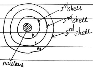
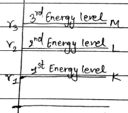
Energy level diagram
Here, above energy level diagram can be only plotted for single isolated atom but in a crystal (solid) there are large number of atoms present which cannot be isolated. Due to electrostatic interaction, the electron in any orbit of such an atom can have a range of energies differing slightly from each other than a single energy value. Hence, a group of energy levels is obtained for a single electron in first orbit. In energy level diagram, it looks like a single line broadened. This broadened energy level is called $$ \underline{\text{Energy Band}} $$.
This energy band play very important role in solids. Some important energy bands are:
(i) Valence band
The range of energy (energy band) occupied by valence electrons is known as valence band. This band may be completely filled or partially filled with electrons depending upon the nature of solids. But it never be empty.
(ii) Conduction band
The range of energy (energy band) passes by the electrons which are just jumped from the valence band is known as conduction band. It may either empty or partially filled. This band plays important role for the conduction of current. If the band is empty then this solid doesn't conduct current but if the band is filled then this solid conduct current. The electrons in this band are called free electrons.
(iii) Forbidden band or band gap
The energy gap between valence band and conduction band is called Forbidden band or band gap. This band gap (difference between valence band & conduction band) gives the required energy value to make electrons free or to make electrons jumps from valence band to conduction band.
Classification of solids (band theory)
On the basis of Band theory, Solids are divided into 3 types:
- Conductor
- Insulator
- Semi-conductor
Conductor
The solids in which valence band and conduction band are overlap to each other or there is no band gap is called conductor. Eg: Na, Mg, Al, etc.
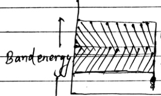
Fig. 1 energy band diagram of conductor.
Insulator
The solid where there is large band gap between valence band and conduction band are called insulators. In insulators the conduction band is completely empty. Due to large band gap (nearly >5.5 eV) high energy (potential difference) is required to make electrons jumps from valence band to conduction band which is practically not possible. e.g. non-metals like diamond, paper, glass, etc.
Fig: energy band diagram of Insulator. (conduction band; Band Gap / forbidden band; valence band)
Semiconductor
The solid having less band gap (nearly equal or less than $$ \pm e $$) are called semiconductor. In semiconductor initially conduction band is empty but after supplying small p.d. it is filled partially. e.g. Si, Ge, etc.
Fig: energy band diagram of semiconductor.
In periodic table IVA group are semiconductors. There is narrow gap between valence and conduction band. The resistivity of semiconductor is in order of $$ 10^{-1}\Omega m $$ where as in conductors resistivity is in order of $$ 10^{-2}\Omega m $$ and on in insulator is $$ 10^{8}\Omega m $$ to $$ 10^{10}\Omega m $$. Resistivity decreases to rise of temperature and at 0K, it becomes perfect insulator.
Generally Silicon (Si) and Germanium (Ge) is used for electronic purpose. The crystal of pure semiconductor is shown in figure below where each semiconductor atom is covalently bonded with other type four semiconductor atoms.
Fig: Silicon crystal
Charge carriers in semiconductor
The charge carriers or the agent due to which current appears in semiconductor is called charge carriers. There are two types of charge carriers in semiconductor: i.e. electrons and holes. When electron jumps from valence band to conduction band, it leaves a vacant space or vacancy of electron in valence band, this vacancy is regarded as holes and it behaves like positive charge. The current in semiconductor is either the flow of electrons in conduction band or the flow of holes in valence band.
To understand the movement of hole, let's see an example of semiconductor.
Due to thermal energy or small p.d., the electron from point 'i' in valence band jump to the conduction band leaving a hole at 'i'. To fill this vacancy, another electron jump from point m to l now the vacancy is shifted to point 'm' again to fill this vacancy another electron from N to M moves again the hole is shifted to point 'N'. Now, the electron from point 'p' jumps to 'N' to fill the vacancy. But the vacancy shifted to point 'p'. Here the electrons moves with path PNML. At meanwhile, holes move with path LMNP i.e. in opposite direction of flow of electron.
Types of semiconductor
Generally the Semiconductors broadly classified into two types.
- Intrinsic semiconductor
- Extrinsic semiconductor
Intrinsic semiconductor
The pure semiconductor crystals are called an intrinsic semiconductor. Eg: Silicon crystal or Germanium crystal due to poor electrical conductivity, intrinsic semiconductor are not so useful.
- Pure form of semiconductor
- It's electrical conductivity is low.
- The number of free electrons in conduction band and the no. of holes in valence band is exactly equal and they are small in number
Examples are crystalline forms of pure silicon and germanium.
Extrinsic semiconductor
The semiconductor having some amount of impurities added or the impure semiconductors are called Extrinsic semiconductors. The addition of proper impurity to pure semiconductor crystal increases the electrical sensitivity of semiconductor So, Extrinsic semiconductors are useful.
- Impure form of semiconductor.
- Its conductivity is high.
- The number of free electrons and holes is never equal. There is excess of e⁻ in n-type semiconductor and excess of holes in p-type semiconductor.
- Examples are silicon and germanium crystals with impurity atoms of arsenic or antimony sodium.
Types of extrinsic semiconductor
P-type semiconductor
- In p-type semiconductor, trivalent impurity like Al, Ga, In, etc. are added.
- Holes are majority charged carriers and electrons are minority carriers.
- The hole density is much greater than the electron density.
- The fermi energy level lies in between the acceptor energy level and valence band.
N-type semiconductor
- In N-type semiconductor, pentavalent impurity like P, As, Sb, Bi, etc are added.
- Electrons are majority charged carriers and holes are minority carriers.
- The electron density is much greater than the hole density.
- The Fermi energy level lies in between the donor energy level and conduction band.